
Finding Equilibrium #12: The world of semiconductors
Hello everyone,
After last issue's semiconductor shortage statistic, I fell down the semiconductors rabbit hole. Given semiconductors underpin all the digital things we do, a 300k semiconductor worker shortage sounded...bad.
But as I dug into the space, I realized how weak my fundamentals were. So I'm going to make this issue a little different. Instead of going broad, we'll narrow in on semiconductors. I'll first take you through my favorite fundamental resources, and then we'll touch on some of today's cool advancements. Many of you are semiconductor experts already, so skip the Foundations to get right to the cool stuff in Advancements! Let's hop right in:
Foundations
This was the most accessible video on the history, fundamentals, and manufacturing processes of semiconductors and microchips. The video lays it out best, but here’s my condensed summary:
Semiconductors are essential because they are the foundation of the microchips that power all our devices. The chip in your phone is only possible because its base is Silicon, a semiconductor.
Semiconductors form the foundation because of their dual property: you can control when it conducts electricity and when it doesn't. That means you can transmit information in the form of electric signals, which unlocks processing capabilities. But to introduce these capabilities to a semiconductor base, you need to add electric components: the main ones are transistors (amplify/nullify signals), capacitors (store energy), and resistors (control current flow). Capacitors and resistors act as moderators, while transistors determine how powerful and fast the chip is.
The importance of the semiconductor base hits home when you look at how these circuits used to be set up. They were an entangled pile of wires hooked up to discrete components. To get more powerful, your "chip" had to enlarge to fit additional transistors and wires. With iPhones having 12 billion transistors, you can imagine how impossible this would've been. But the discovery of semiconductors eliminated this need for discrete components: instead of wiring components together, they could be "etched" onto a semiconductor base! Wires and components were essentially turned into lines on a Silicon base. Everything was in one place: it was an integrated circuit (IC).
ICs made individual chips possible because they opened up the design space by removing the size constraint. Without needing wires and discrete components, chip performance and size didn't need to be proportional. Semiconductor professionals could focus on making components smaller in the interest of performance, not just to make size manageable. This kicked off Moore's Law, where the number of transistors in an integrated circuit doubled every two years (i.e chip performance doubles every two years).
And that brings us to today. Transistors per chip have increased exponentially, enabling us to have everything from cloud computing to AI and our cellphones. But while more transistors means more performance, it also creates an ever-growing design problem: where do we place them on the chip? If you've got billions of transistors, that's a crazy high number of possible combinations. Today's focus is solving this exact problem, the chip placement problem.
Improving a chip's processing power isn't just about jamming more transistors into it. Instead, you've got to maximize performance while minimizing power consumption and area (PPA). You also can’t just squeeze all the components too close together. It turns out that if transistors are too close, you run the risk of congestion and short circuitry. So we’ve got a problem. Chip area is decreasing, the number of components (and so potential combinations) is increasing, and PPA demands are growing tighter. There's also the advent of specialized chips (for example, there are AI chips, Data Center chips, etc.), which adds yet another dimension to chip design.
Put a worker shortage together with this increased complexity, and it's clear humans need some help. We need to be able to do more with less. As you’ll soon see, that’s where a ton of cool AI research is making big strides!
Before we jump into the cooler stuff, if you're curious on how chips are manufactured or want to dig deeper into ICs, I found these 3 resources enormously helpful:
Explain That Stuff: We've established that a microchip is just an IC. An IC packages together all the individual components onto one integrated chip. This article simplifies that and drives the concept home.
Britannica: Integrated Circuits: This goes one level deeper into ICs by providing an overview of different IC types. The most relevant are microprocessors and ASICs. Microprocessors are complex and flexible, they unlocked the computer revolution. ASICs are less flexible but more focused, they're usually used in high-compute, narrow processes, like bitcoin mining. The main takeaway is that there are 1000000s of ways to design different ICs – they all revolve around how we place and connect components.
(ASML) How Microchips are made: I didn't cover manufacturing , but the microchip manufacturing process is insane. ASML is a vital equipment provider for it too – they make the machines that laser the components onto the semiconductors. The 11-step graphic on this link is a phenomenal and accessible overview of the end-to-end process.
The Cool Stuff: Advancements
Forbes summary: A lay of the land
We've determined why semiconductor/chip design is intricate: you're trying to fit billions of shrinking components onto an ever-shrinking base while making sure it's powerful, fast, and cheap. It's physically impossible for a human to do this with billions of transistors, but luckily we've had software's help. But that help needs to be a lot more advanced soon. This Forbes article gives an overview on how AI is filling that gap, with the following diagram being particularly handy in mapping out how to navigate semiconductor design:
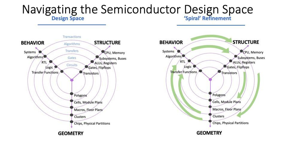
The chip design process cycles through 3 phases:
Behavior (what the chip should do)
Structure (how the chip will do it)
Geometry (where to place things on the chip)
If you start on the outer circle at behavior and spiral your way clockwise down to the middle, you have the cycle of steps in chip design. Most of today's innovation is around Geometry, figuring out chip placement, but behavior changes are now triggering structural changes too. For example, we expect more from our phones today than 10 years ago. That behavioral change triggered a change in what those chips should do. Changing what a chip does sets off changes in how the chip accomplishes that and its lower-level design – that's why Apple has it's own chips for all its devices. It required a complete redesign from the ground up. This same specialization is occurring all over the place, and is only accelerating.
Chip Design with Reinforcement Learning
Here's Google's summary on how they're solving for chip design with AI. It's focused on the "Geometry" area above. They do a great job of distilling both the problem space and their solution, especially how it shortens chip design from 2-5 years to a few months.
The crux of their innovation is continuously using Reinforcement Learning to improve chip design. Reinforcement Learning is a type of Machine Learning that constantly learns from outputs, instead of being trained once and deployed. So rather than being given the answer sheet upfront, it continuously rearranges components on a chip to find what works best.
What's exciting is that Google's model draws parallels between many different problem spaces, making it increasingly generalizable. So while this research focused on a specialized chip (Google's TPUs for AI processing), it's showing signs of working in other chip forms too! If we're running out of people and chip design keeps getting harder, solutions like this will be vital.
Here's another Google example, but focused on the "Structure" area in the design diagram. Instead of focusing on how to lay components on the chip, this effort explores different architectures for specialized use cases. It's another hairy optimization problem: the search space is exponentially large (tweaking parameters like memory capacity, compute core counts, etc.) while the target outcomes (low latency, energy efficiency, etc.) are nuanced and narrow. As our online behavior evolves, research like this will also play an important part in linking behavior to design through optimal architectures.
On the topic of structure, NVIDIA has been making leaps. They released their new chip with 80 billion transistors: the NVIDIA H100 Tensor Core GPU. It's designed for data centers, particularly around accelerating highly intensive AI workloads. If you scroll through their product page, there's tons of ways they've rearchitected how a chip works to make this happen. As design tools improve, this is a (rather extreme) example of what more companies can achieve in the future. As tools become more powerful and accessible, smaller companies will be empowered to achieve similar feats for different niches. What also makes this possible is the fact that companies don’t have to have their own manufacturing facilities. NVIDIA doesn't manufacture any of their chips – they have all the cool toys to advance design and simulation, but then hand it off to their manufacturing partner, TSMC, to build it out!
Synopsis launches it's SaaS offering
While less crazy than the Google research, this is a massive shift in accessibility. Synopsis is one of the big players in the chip design space with its EDA – an Electronic Design Automation solution. By migrating to the cloud and offering their EDA as a SaaS tool, they've lowered the barrier to people using it. Chip designers don't have to worry about cumbersome installations or the computing infrastructure needed to run their simulations, they can pop up their browser, input requirements, and pay for the compute they use. It also means Synopsis can release features faster. With more speed and users, Synopsis could play a key role in reinventing chip design and bringing in new waves of semiconductor designers!
I know this has been a long one, so I'll cut it short here. Hopefully that gave you a flavor for semiconductors and some crazy changes coming our way. Thank you for spending (more than) a few minutes with me, I’ll be back to the usual structure next time!
See you next time,
Aqil